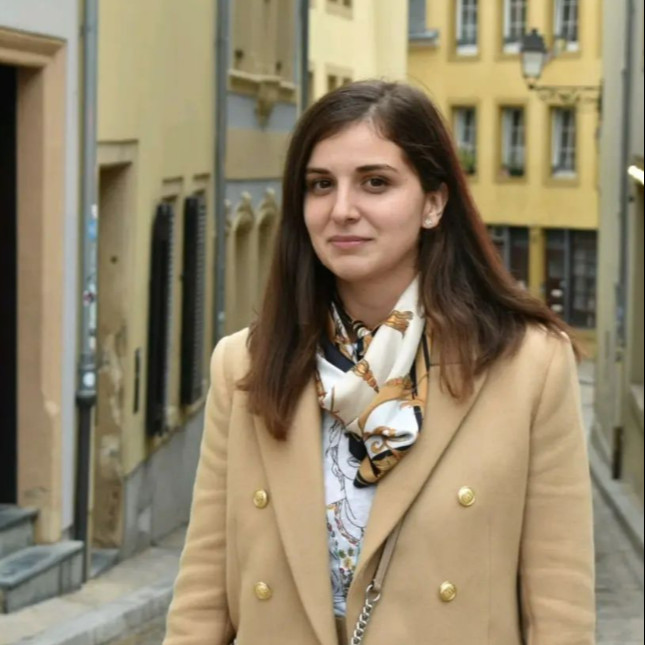
I am a Process Scientist with an experise in Nanotechnology working on Advanced Packaging at Besi Semiconductors, NL.
Completed PhD at the University of Birmingham, UK and a PostDoc from TU Delft, NL.
I was born on 1st of November 1992.
1999-2007 Primary School Safvet-Beg Basagic
2007-2011 High School First Bosniak High school (department: natural sciences and mathematics)
2011-2015 Bachelors program; Theoretical Physics; Bachelors thesis: "Application of saffle point method for a high harmonics generation of hydrogen atoms."
2015-2016 Masters program/Internship in TNO institute, Holst centre, Netherlands: Experimental physics; Masters thesis: "Spatial Atomic Layer Deposition (s-ALD) of InZnO thin films for Thin Film Transistors (TFTs)." Published a publication.
2017-2021 PhD in Solid State Physics; University of Birmingham, United Kingdom; PhD thesis: "Synthesis, processing and morphological properties of highly porous supercritically dried mesoporous silicon nanostructures for drug delivery applications"; 2018 Moreton Award; a worlds record in the highest volume of porosity of porous silicon, 92.3% porosity. Published many publications on this and other topics of my PhD programme.
2021-2023 Postdoc in Porous nanomaterials in Batteries application; Technical University Delft;
2023-2026 Materials Research Scientist in Shell, Future technologies, Amsterdam.
from 2026 - Process Scientist at Besi Semiconductors.
I work and live in the Netherlands. In my free time I do lots of sports, such as cycling, spinning, running, bouldering, yoga and gym classes. I run halfmarathons but I am planning to do a full marathon in the coming years. I take Dutch course and I am actively and intensively learning it. I really love to travel and on a yerly basis I do lots of trips around the world.
A range of the distinctive physical properties, comprising high surface-to-volume ratio, possibility to achieve mechanical and chemical stability after a tailored treatment, controlled quantum confinement and the room-temperature photoluminescence, combined with mass production capabilities offer porous silicon unmatched capabilities required for the development of electro-optical devices. Yet, the mechanism of the charge carrier dynamics remains poorly controlled and understood. In particular, non-radiative recombination, often the main process of the excited carrier's decay, has not been adequately comprehended to this day. Here we show, that the recombination mechanism critically depends on the composition of surface passivation. That is, hydrogen passivated material exhibits Shockley-Read-Hall type of decay, while for oxidised surfaces, it proceeds by two orders of magnitude faster and exclusively through the Auger process. Moreover, it is possible to control the source of recombination in the same sample by applying a cyclic sequence of hydrogenation-oxidation-hydrogenation processes, and, consequently switching on-demand between Shockley-Read-Hall and Auger recombinations. Remarkably, irregardless of the recombination mechanism, the rate constant scales inversely with the average volume of individual silicon nanocrystals contained in the material. Thus, the type of the non-radiative recombination is established by the composition of the passivation, while its rate depends on the degree of the charge carriers' quantum confinement.
Biodegradable porous silicon (pSi) particles are under development for drug delivery applications. The optimum particle size very much depends on medical use, and microparticles can outperform nanoparticles in specific instances. Here we demonstrate the ability of sedimentation to size-select ultrasmall (1–10 μm) nanoporous microparticles in common solvents. Size tunability is quantified for 1–24 h of sedimentation. Experimental values of settling times in ethanol and water are compared to those calculated using Stokes’ Law. Differences can arise due to particle agglomeration, internal gas generation and incomplete wetting. Air-dried and supercritically-dried pSi powders are shown to have, for example, their median diameter d (0.5) particle sizes reduced from 13 to 1 μm and from 20 to 3 μm, using sedimentation times of 6 and 2 h respectively. Such filtered microparticles also have much narrower size distributions and are hence suitable for administration in 27 gauge microneedles, commonly used in intravitreal drug delivery.
Porous silicon layers on wafers are commonly converted into particles by mechanical milling or ultrasonic fragmentation. The former technique can rapidly generate large batches of microparticles. The latter technique is commonly used for making nanoparticles but processing times are very long and yields, where reported, are often very low. With both processing techniques, the porosity and surface area of the particles generated are often assumed to be similar to those of the parent film. We demonstrate that this is rarely the case, using air-dried high porosity and supercritically dried aerocrystals as examples. We show that whereas ball milling can more quickly generate much higher yields of particles, it is much more damaging to the nanostructures than ultrasonic fragmentation. The latter technique is particularly promising for silicon aerocrystals since processing times are reduced whilst yields are simultaneously raised with ultrahigh porosity structures. Not only that, but very high surface areas (> 500 m2/g) can be completely preserved with ultrasonic fragmentation.
In this manuscript, the authors investigate the growth of indium zinc oxide, indium zinc oxide (InZnO, IZO) as a channel material for thin-film transistors. IZO is grown at atmospheric pressure and a high deposition rate using spatial atomic layer deposition (S-ALD). By varying the ratio of diethylzinc and trimethylindium vapor, the In/(In þ Zn) ratio of the film can be accurately tuned in the entire range from zinc oxide to indium oxide. Thin film transistors with an In to Zn ratio of 2:1 show high field-effect mobility—exceeding 30 cm2/V s—and excellent stability. The authors demonstrate large scale integration in the form of 19-stage ring oscillators operating at 110 kHz. These electrical characteristics, in combination with the intrinsic advantages of atomic layer deposition, demonstrate the great potential of S-ALD for future display production.
Ova stranica koristi kolačiće da bi vam pružila najbolje iskustvo
Saznaj više